PhotonSharpBeta v0.1 Open PhotonSharpOpen app

PHOTONSHARP · SILICON PHOTONICS IDE

Free for all -
photonics made easy

Design silicon chips, from design to manufacture

Write optical programs, inspect the circuit they generate, run simulations, and prepare designs for fabrication review in one workspace.

Free account · 250 MB project storage · No payment required · System requirements ↗

PhotonSharpBeta v0.1PhotonSharp — Demo
λλ Code⑂ Program flow⬡ Circuit designer▷ Results▱ Layout▧ Fabrication
EXPLORER⌄ Workspaceλλ  demo.photon▤  process-spec.jsonCIRCUIT ELEMENTS◇  Input port⋈  Couplerφ  Phase shifter◎  Output port
⬡  Circuit designer · demo.photon▶ Simulate
◇IN 1
◇IN 2
⋈COUPLER
φPHASE
◎OUT 1
◎OUT 2
✓ Circuit ready · 6 elements · 5 connections λ 1550 nm

Drag optical components into a circuit, then refine the λλ source.

WRITE λλ CODEGENERATE CIRCUITSSIMULATEPREPARE LAYOUTREVIEW FAB SPECS

01 / ONE CONNECTED WORKFLOW

An idea in code.
A circuit you can see.

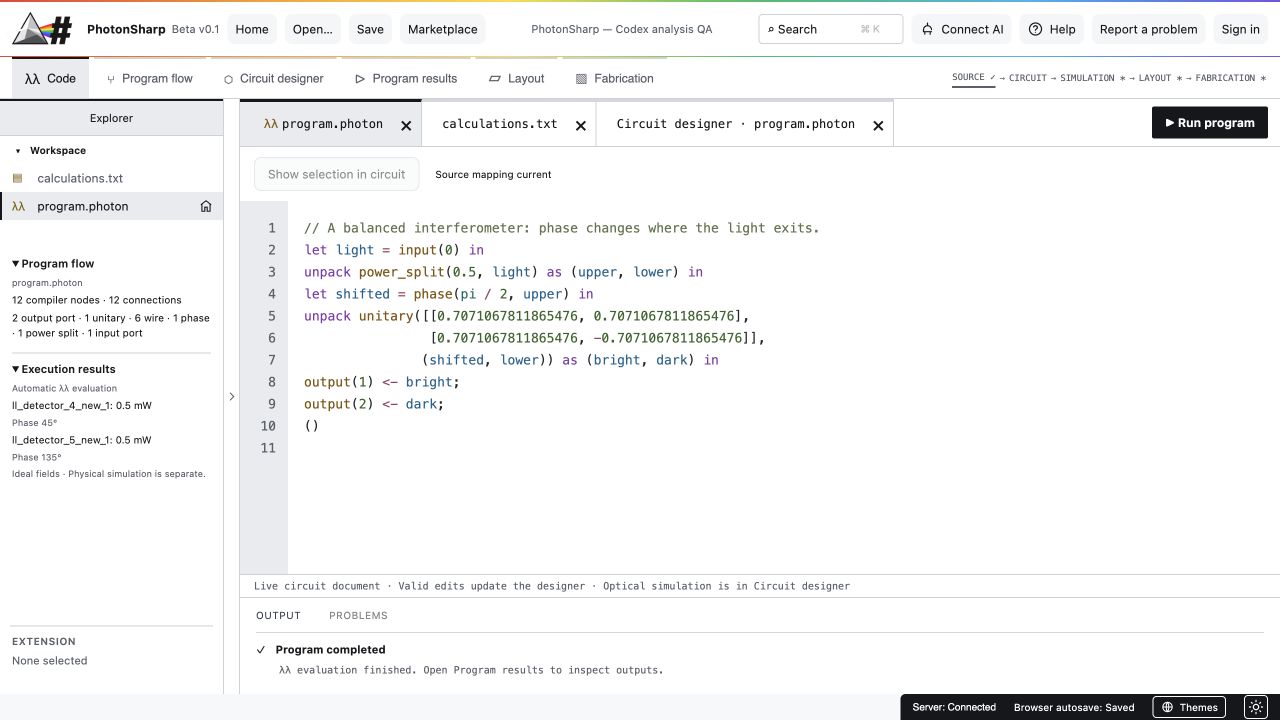
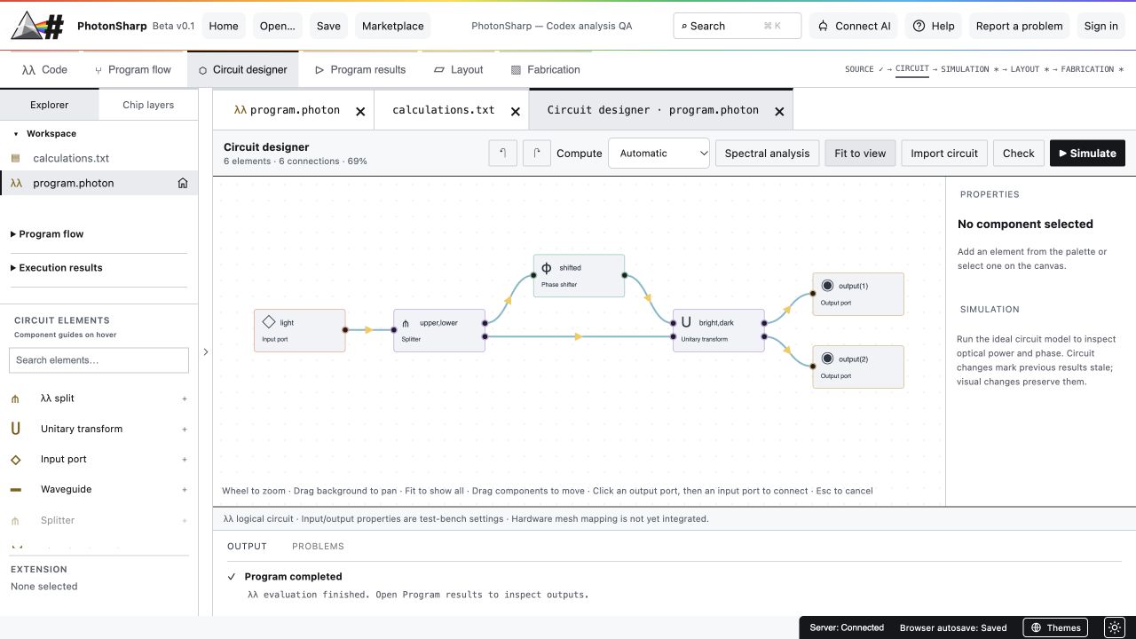
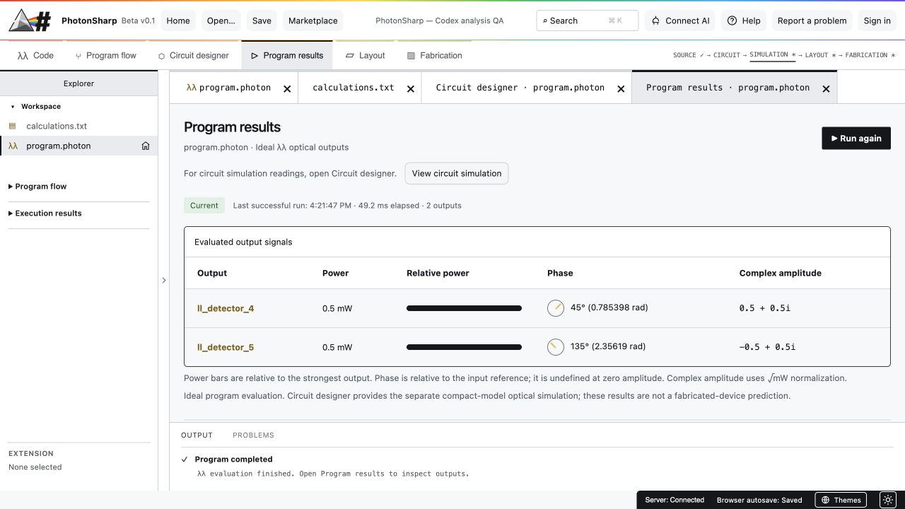
Follow the same interferometer from its first line of λλ to its optical outputs. Explore the actual editor, with every step in the same workspace.

PhotonSharp editor with the complete interferometer λλ program
Actual workspace · λλ source Learn the language ↗

Write signal expressions. PhotonSharp generates the components and their connections.

Download the example ↓Open the editor ↗

02 / GET A FEEL FOR PHOTONICS

A small change.
A different path for light.

Change the phase on one arm of an ideal interferometer. The two waves combine differently, moving optical power between its outputs.

INTERFEROMETERInteractive illustration
◇⋔φU◎◎ 1 mW inputsplitphase shiftcombineoutput 1output 2
let shifted = phase(pi / 2, upper) inλλ
TRY IT YOURSELF

Turn the phase.
Watch the outputs.

0°180°360°
Output 10.50 mW
Output 20.50 mW

Ideal, lossless illustration with a 1 mW input. This is a teaching example, not a device prediction.

03 / LOOK BEYOND ONE READING

See the response.
Find the next question.

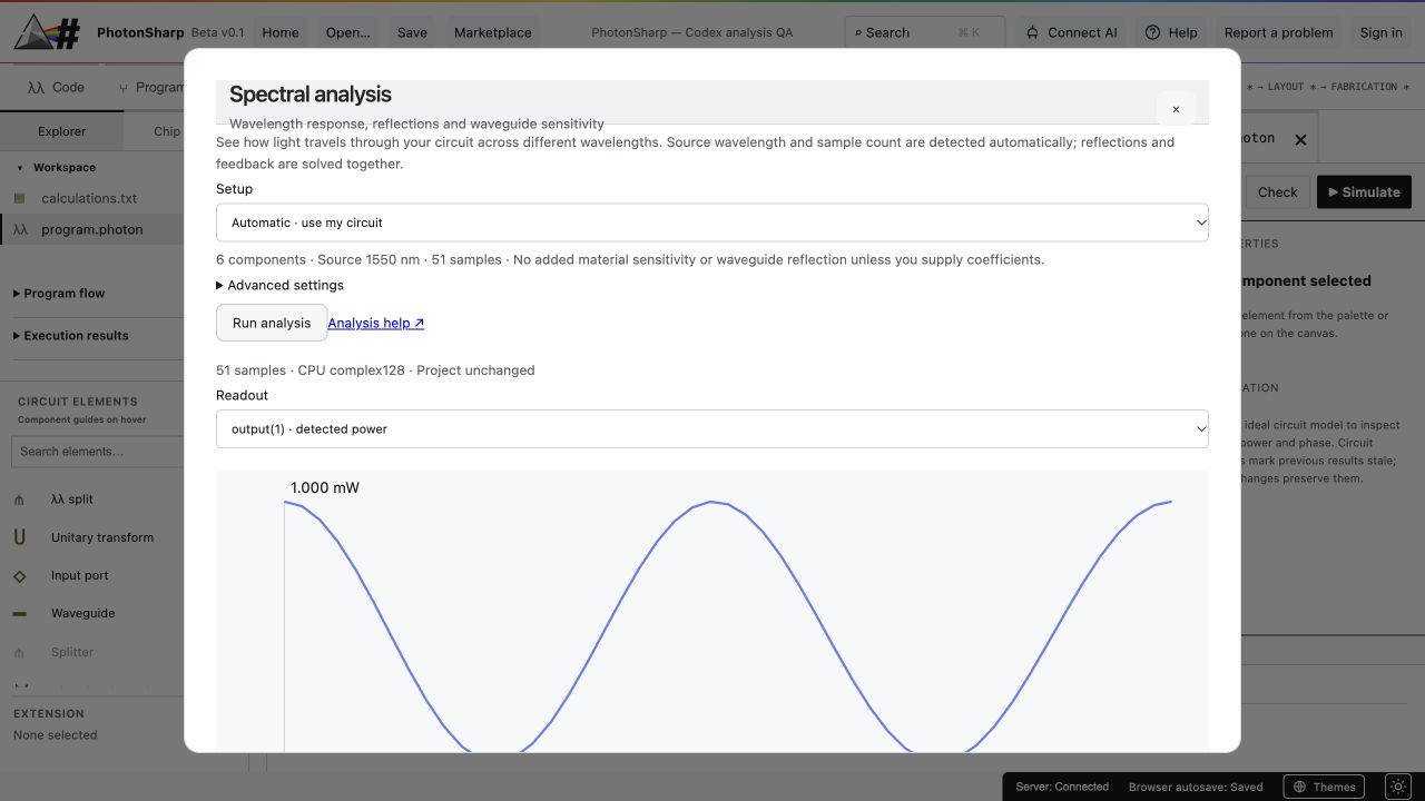
Sweep wavelengths through a supported linear circuit. Inspect detector power, reflected light and feedback, with automatic settings to get you started.

  • Source wavelength detected automatically
  • Sample count matched to circuit size
  • Detector readout selected for you
Explore spectral analysis ↗

Material sensitivity uses coefficients you supply. The linear solver does not support Kerr components.

Real PhotonSharp spectral analysis showing automatic setup and a wavelength response plot
Actual workspace · Spectral analysis
REPLAY SOLVER READINGS
1500 nm1600 nm1 mW

1500 nm · 1.00 mW

Actual linear-solver samples · 20 µm waveguide in one arm · 1 mW input

04 / KEEP THE WHOLE DESIGN TOGETHER

Less setup.
More room to explore.

Start with a small optical experiment. Keep the tools for your next step close by.

PHYSICAL LAYOUT

A first step toward real geometry.

Generate supported generic SOI cells, route optical ports and run basic waveguide width and spacing checks. Export geometry for development and review.

See the layout workflow ↗Generic development process. Full foundry verification is still required.
LANGUAGE + EXTENSIONS

Signals first. Connections follow.

Learn λλ, then add optical operations such as waveguides, couplers, probes and detectors. Find signatures and examples in the searchable reference.

Browse the language reference ↗
PROJECTS + YOUR AI

Your work, with its context.

Save and share projects from your account. Connect your own AI client with project-scoped MCP access and a private configuration you control.

Learn about projects and sharing ↗

YOUR NEXT EXPERIMENT STARTS HERE

Make room for
your next bright idea.

Free to use in your browser. A free account includes 250 MB of project storage.

Start designing ↗Build your first circuit →

A FEW THINGS TO KNOW

Before you begin.

Do I need to install anything?

No. PhotonSharp runs in a desktop browser. Open the workspace on your computer; the editor is not available on phones. See the system requirements for details.

What can I simulate?

Run ideal λλ program evaluation, or use separate linear spectral analysis for wavelength sweeps, specified reflection and feedback. Timing, noise and full electromagnetic field solving are not included. Kerr behavior in the ideal evaluator is illustrative and uncalibrated.

Can I manufacture a chip from it?

The generic SOI workflow generates development geometry and runs basic waveguide checks. Manufacturing still requires a compatible foundry PDK, calibrated models, full physical verification and foundry approval. Passing a generic check is not tape-out signoff.

Can I get more project storage?

Paid checkout is not open yet. The planned 10 GB plan is $2.99/month. Larger 100 GB and 1 TB plans are available on request. Contact [email protected].